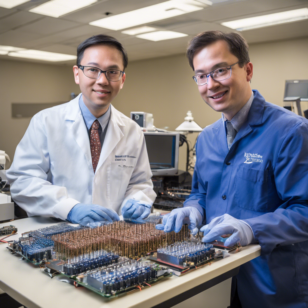
Penn State Researchers Achieve Breakthrough in 3D Integration of 2D Transistors

Advancements in monolithic 3D integration using 2D materials pave the way for smarter and more versatile electronic devices.
Moore’s Law, the principle that predicts the doubling of transistors on a chip every two years, has driven the rapid advancement of computing power. However, the physical limitations of cramming more transistors into a confined space have posed challenges for further progress. In a groundbreaking study published in Nature, researchers from Penn State University propose a solution: the seamless implementation of 3D integration with 2D materials. This approach not only allows for the packing of more transistors onto a computer chip but also enables the incorporation of diverse functionalities within different layers of the stack. The researchers demonstrate the feasibility of this approach, opening up new possibilities for electronic devices.
Monolithic 3D Integration: More Moore and More than Moore
The concept of 3D integration involves vertically stacking multiple layers of semiconductor devices. This approach, known as “More Moore,” increases the density of transistors on a chip. Additionally, it allows for the use of transistors made from 2D materials, leading to the concept of “More than Moore,” which involves incorporating diverse functionalities within the stack. The researchers at Penn State demonstrate the potential of monolithic 3D integration, a fabrication process where devices are directly made on top of each other, as opposed to stacking independently fabricated layers.
Overcoming Challenges with Temperature
While monolithic 3D integration offers numerous advantages, it also presents significant challenges. Conventional silicon components used in the process have a limited temperature tolerance, making it difficult to achieve the desired integration. However, the use of 2D materials, such as transition metal dichalcogenides, overcomes this obstacle. These materials can withstand the temperatures required for the process, enabling researchers to achieve monolithic 3D integration at a lower temperature than traditional silicon chips.
Energy Efficiency and Distance Reduction
Vertical stacking in 3D integration not only increases transistor density but also improves energy efficiency. By reducing the distance between devices, the researchers were able to decrease lag and power consumption. This achievement aligns with the “More Moore” criterion. Additionally, by incorporating transistors made with 2D materials, the researchers met the “More than Moore” criterion. The unique electronic and optical properties of 2D materials, including sensitivity to light, make them ideal for sensors. As the number of connected and edge devices continues to grow, the ability to add new functionalities to electronic devices becomes increasingly important.
Advantages of Using 2D Devices for 3D Integration
Using 2D devices in 3D integration offers several advantages. These devices have superior carrier mobility, enhancing the efficiency of electrical charge transport in semiconductor materials. Additionally, their ultra-thin nature allows for more transistors to be fitted on each tier of the 3D integration, leading to increased computing power. The researchers’ achievement of 3D integration at a massive scale, characterizing tens of thousands of devices, bridges the gap between academia and industry.
Conclusion:
The breakthrough achieved by Penn State researchers in 3D integration using 2D materials paves the way for the development of smarter and more versatile electronic devices. By overcoming the limitations of conventional silicon chips and leveraging the unique properties of 2D materials, the researchers have demonstrated the feasibility of monolithic 3D integration. This advancement not only enhances the density and energy efficiency of electronic devices but also enables the incorporation of diverse functionalities. As the research progresses, Penn State aims to lead the way in partnering with the semiconductor industry to further advance this technology. The potential impact of this breakthrough on the future of electronics is significant, promising a new era of computing power and functionality.

